Band Structure Of P-N Junction Semiconductor
Di: Everly
This outer shell of a semiconductor or insulator is known as the valence band and includes electrons that are bound to the atom. The valence electrons participate in bonding to other
For a p-type semiconductor . In these semiconductors, a very small supply of energy can cause an electron from its valence band to jump to the acceptor energy level. The
9.11: Bonding in Semiconductors
Presently, Those 2D materials used in state-of-the-art electrical and optoelectronic devices because of the extensive nature of their electronic band structure. 2D materials offer
Although a few devices can be made from such semiconductors, the majority of devices and the most important ones utilize nonhomogeneous semiconductor structures. Most
Download scientific diagram | Band structure of energy levels-(a) semiconductor type P, N, (b) not illuminated PN junction, and (c) illuminated PN junction from publication: Temperature
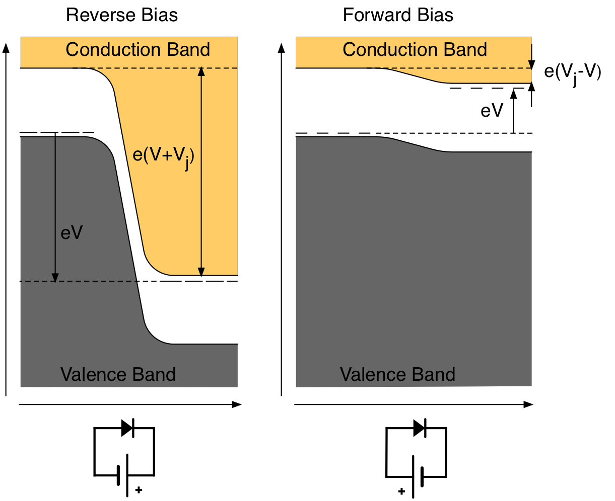
An energy diagram for a pn junction at the instant of formation is shown in Figure (a). As you can see, the valence and conduction bands in the n region are at lower energy levels than those in
- Formation of pn junction and its band diagram
- Semiconductor materials: pn junction Contents
- ProblemsandSolutionsto PhysicsofSemiconductorDevices
As a result, the charge density of the P-type along the junction is filled with negatively charged acceptor ions ( N A ), and the charge density of the N-type along the junction becomes
Learn how to build a p-n junction device. Learn how to study the current-voltage characteristic of such a device. Compare two different methods: ATK-SE and ATK-DFT. Analyze the electronic
The aim of this chapter is a discussion of the physics of a semiconductor p-n junction, i.e., a semiconductor structure in which there is a change from n type to p type over some region of
Energy Diagrams of PN Junction & Depletion Region
The panels show energy band diagram, electric field, and net charge density. The built-in potential of the semiconductor varies, depending on the concentration of doping atoms. In this example, both p and n junctions are doped at a 1e15 cm
LEDs are p-n junction devices made from extrinsic semiconductors. An n-type and a p-type semiconductor are put in contact with each other to form a p-n junction diode. The difference in
By extending our examination to a crystal composed of N atoms, each with a single electron, we observe an interesting process: the initial \(n=1\) energy level splits into N
If the band gap is sufficiently small to allow electrons in the filled band below it to jump into the upper empty band by thermal excitation, the solid is known as a semiconductor.In contrast to
Equilibrium band structure of Mn(Bi 1−x Sb x) 6 Te 10 with x = 0.18. (a) Band structures along the Γ–M direction on the MBT and 1-BT terminations. (b) Hall measurements
In the band diagrams for the metal contacts with n- and p-type semiconductors, you see from the bending of the vacuum potential energy that in the n-type case, an electrical
- Semiconductor Energy Bands
- Basic Structure of PN Junction in Semiconductor:
- Understanding Open-Circuited P-N Junctions in Electronic Circuitry
- Lecture 12: Photodiode detectors
The second building block is the p-n junction, a junction of p-type and n-type materials indicated in Figure (3b). The p-n junction is the key compound for numer-ous semiconductor devices. By
As the name suggests, a p-n junction depicts the combination of two semi conductors having n- and p-type conductivities. If the two semiconductors forming the junction are of the same
Effect of surface states on band structure. (a) Semiconductor without any surface states and hence no Fermi-level pinning. (b) n-type semiconductor with a depletion region and
The fundamental building block of all semiconductor devices is the p-n junction. Its primary electrical characteristic is that it allows current to flow easily in one direction only. The
Junction photodiodes The semiconductor photodiode detector is a p-n junction structure that is based on the internal photoeffect. The photoresponse of a photodiode results from the
A hybrid tin-based perovskite solar cell with p-i-n inverted structure is modeled and simulated using SCAPS. The inverted structure is composed of PEDOT:PSS (as hole transport
2 Aim: To determine the Energy Band Gap of a Semiconductor by using PN Junction Diode. Apparatus: Energy band gap kit containing a PN junction diode placed inside the temperature
Exploring the energy band structure of an unbiased P-N junction is the root of grasping how electrons and holes interact within semiconductor materials. Basic to this understanding is the
Download scientific diagram | Energy band diagram of PN Junction under Equilibrium from publication: P-N Junction | It can be quite confusing to study the PN junction with all its differential
The second building block is the p-n junction, a junction of p-type and n-type materials indicated in Figure (3b). The p-n junction is the key compound for numerous semiconductor devices. By
electrons fill 4 bands made of s and p orbitals Band Structure of Semiconductors EF Electrons are only excited in a very limited region of energy Plot Energy versus k. EF separates filled and
band structure with an energy gap between valence and conduction bands of the order of ∼ 1eV. Figure 1 schematically illustrates this basic structure consisting of a valence band,
Semiconductors. Semiconductors are defined by their name: they are kinda conductive. These materials have a band gap, but it’s not as big as that of an insulator.Often in the field, \(3
Figure 3.2 depicts the various structures of junctions in semiconductors with different band gaps. Let us discuss the junction region where mainly a p-n or n-p junction is fabricated. The active
The band gap of a semiconductor is the minimum energy required to excite an electron that is stuck in its bound state into a free state where it can participate in conduction. The band
DEMONSTRATIONS PROJECT. Band Structure of P-N Junction Semiconductor
Basic Structure of PN Junction in Semiconductor: Most semiconductor devices employ one or more P-N junctions. The P-N junction is the control element for the performance of all
- Welcome Center Essen Termin _ Ausländerbehörde Essen Termin Online Einbürgerung
- Checkered Flag Svg: Checkered Flag
- Motorkennfelder Für Verluste Erstellen
- Wie Lange Fliegt Man Von San Francisco Nach New Orleans?
- Neuseeland: News Und Hintergründe
- Marktforschung Jobs Und Stellenangebote In Gutenacker
- Sanitätshaus Ihr Gesundheitsteam Helmstedt
- Studieninhalte Master Medien Und Digitale Kulturen
- Camping Les Méditerranées Beach Garden 5* À Marseillan
- Klein, Aber Oho: Das Sind Die Kleinsten Profi-Fußballer Der Welt!
- Outdoorfliesen/Ausstellung/Fliesen Heidbrink Kirchhorst
- Davina Geiss Scroller